PCB design with DipTrace
Continuing from part 1 of this ATtiny2313 breadboard header with DipTrace -tutorial, I’ll now go through the PCB design. In DipTrace Schematic Editor, I used File->Convert to PCB (CTRL-B) to get the components and connections exported to PCB Layout tool. Like it’s schematic counterpart, also this tool is quite easy to use.
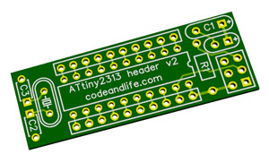
First I change the grid to 5 mil so each step is half of the 10 mil breadboard hole spacing. I then proceed arrange the components roughly to final layout, and add two 10-pin headers which will plug into breadboard. I then remove some component names which are not sorely needed, and change the location for the remaining ones to the center of the component.
Spacebar is again used to rotate components 90 degrees, and multiple items can be selected with ctrl+click. You probably notice that at some points of the video, the popup-menu options go outside the recording area. Sorry for that! However, I trust you’ll be able to find the correct option yourself if you look at the window that then pops up – usually it’s “xxx properties”, like component or pad properties that I open.
After getting the components more or less to their correct locations, I then draw a board outline (after adjusting the grid to a slightly fines 2.5 mil pitch). DipTrace also has an excellent “Replace pattern” option that lets me change the pattern used for a given component, which I used to replace crystal capacitor patterns with one that takes up less space on silk screen (the distance between pads stays the same, though).
The most important and many times the hardest part of the PCB design is routing. DipTrace has an autoroute option, but it doesn’t do as good job as a human would – I tried it and while it worked OK, it had to make one or two vias (metal-filled holes that go through the PCB to enable a trace to go from one side to another outside the component mounting holes). After some head-scratching, I managed to figure out a way to avoid vias completely, and this is what I use here. I Before routing, I tweak the component locations a bit, and make the header holes and pads slightly larger (square header pins require slightly larger holes than normal through-hole components). Note that “T” and “B” keys toggle between top and bottom signal layer!
As you can see, I configured the trace options so that VCC trace is a bit thicker – GND is a smaller issue, as I’m using ground copper pour which should fix that later on. If you look carefully through the video, you’ll notice that I still had the crystal capacitors turned the wrong way, and at 3:06 the software asks if I really want to merge two nets that were previously unconnected. This was thankfully quick to fix. Towards the end, I also make one more tweak so the crystal caps have square pads for positive terminals (it just looks slightly better even though ceramic capacitors are not polarized :)
The final video shows how I add a copper pour on the bottom layer. I chose a solid fill and to remove unconnected islands of copper. You can get my “production version” PCB file, which has a grid fill for the pour, as well as some other tweaks to pass Olimex fab requirements.
Proceed to part 3: Manufacture tweaks and Gerber creation process
