World’s Simplest Logic Analyzer for $5
Today’s post documents my recent hack that may just be the world’s simplest logic analyzer. More accurately, it is a circuit consisting of a 74HC126 quad buffer chip and R-2R resistor network (eleven 330 ohm resistors) that acts as a D/A converter, enabling one to analyze four logic lines with a single channel digital oscilloscope and $5 in parts!
With the circuit described below and an entry level USB scope like the PicoScope 2204, bursts of data can be captured at 10 MSps (million samples per second), and continuous capture rates of 2.5 MSps are possible, the length of the capture only limited by your PC’s memory. This is obviously much better than recently covered Bus Pirate’s 1 MSps for 4 ms!
Even higher throughput can be achieved with better scopes, although the A/D conversion requires several consecutive samples at same logic level, which means that a 100 MHz scope with 200 MSps capture rate should generally be able to analyze logic operating at ~40 MHz speeds. At such speeds, a fast buffer chip and D/A converter is naturally needed as well.
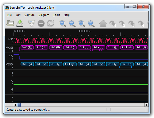
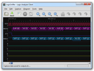
Above you can see an example of SD card traffic analyzed using my circuit – the full capture was 10 million samples which enabled me to capture all the traffic generated by my SD tutorial project without any additional triggering. Read on for details of the hack. A lot of effort has been made to keep the material very accessible and informative to electronics beginners, too. In the end of the article, source code for PicoTech 2000 series is included, and it can easily be adapted for any scope that can transfer captured waveforms to PC (in the simplest form by reading waveforms from a CSV file).
How It Works
Basic idea is to connect 4 logic lines to a D/A converter, that will transform the binary 1/0 values (represented by VCC and GND voltage levels, respectively) into a 16-step analog waveform. Because input lines cannot be directly connected to the R-2R resistor network that is used to do the D/A conversion, a 4-line buffer chip is used in between to provide high impedance inputs that do not interfere with the logic being analyzed.
From logic levels to 16-step analog signal
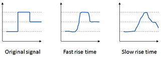
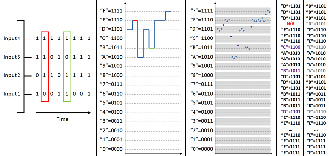
From the buffer chips I had at my disposal, I selected the 74HC126 quad buffer. It had a short propagation delay, and even more importantly, very impressive change times between logic levels – just a few nanoseconds from LOW to HIGH and vice versa. This is important, because the analog signal is later converted back to logic levels, and the shorter the transitions, the easier it is to deduce the original shape, as illustrated in above diagram.
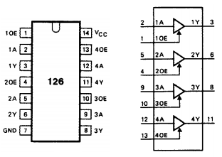
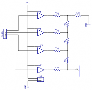
The 74HC126 buffer is a very simple beast – there are connections to ground and VCC, and four “output enable” pins which need to be held high to enable the outputs (in otherwise identical 74HC125, the enable pins are active low). The inputs 1A-4A are connected to device being analyzed, and the outputs 1Y-4Y are connected to the R-2R network that acts as a D/A (digital to analog) converter. 74HC family can be powered from anything between 2 and 6 volts, which makes it a good choice for analyzing circuits at various operating voltages. The full schematic can be seen below.
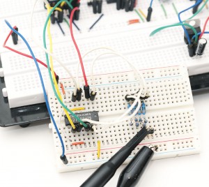
I wired the project on a small breadboard, using two small 330 ohm resistors side-by-side to get fairly close to 115 ohm resistance. I then programmed one of my ATmega chips to generate a repeating signal from four of its pins and connected my Picoscope to the point marked with “OSC” in the schematic to see it was functioning as it should.
The circuit can also be checked with a voltmeter alone: All inputs low (connected to GND) the voltage between “OSC” and GND should be 0V. When input 1 alone is high (connected to VCC), the voltage should rise to 1/16th of VCC (assuming GND=0V). For input 2 it’s VCC/8, for input 3 it’s VCC/4, and for input 4 it’s VCC/2. Finally, all lines high results in the sum of those four, i.e. 15/16 * VCC.
From analog signal back to logic levels
Above you can see different phases of the conversion process the signal goes through. First, the D/A conversion discussed in the previous section combines the ones and zeroes (VCC and GND level voltages) in four input lines into a single analog signal with 16 separate levels, 0V corresponding to “all zeroes” and 15/16 VCC to “all ones”. Two different time points are highlighted to illustrate how the bit values define the voltage level. Of course, due to imperfections in components, the actual signal is not as clean as in the square image.
After the signal has been converted to analog form, the oscilloscope is then used to sample that signal. This phase adds additional noise, and the amount of data points available per time unit depends on the sampling rate. For example, if the logic levels at inputs were changing at the rate of 100 kHz, a sampling rate of 1 MSps would provide 10 samples on average per “logic state”.
To convert the voltage measurements back to original logic levels, we need to know the expected average voltage level of each of the 16 different levels generated by the D/A conversion, and create “windows” around these averages. In the diagram above, these windows are represented by gray rectangles – any data points falling within these windows are interpreted as that level. A small gap is left between the windows, as values around the gaps might be from either of the adjacent windows (due to noise).
Also note that when voltage drops from “E” to “A” for example, it will briefly go through all the values between them (“D”, “C”, and “B”). If the oscilloscope measures a value during this transition, we will get a “glitch” in the data, i.e. an invalid reading. Depending on sample rate, the reading may be wrong for one or several samples. To eliminate these glitches and remove unknown values, the “raw conversion data” is filtered to remove values outside the windows or values that do not stay in the same window long enough. The “raw data” and filtered dataset is shown in the two rightmost columns of the above diagram.
After this filtering process, we can easily deduce the original logic states of the four input lines, and see that the circuit connected to the logic analyzer (on the left) was sending 0xDEADBEEF (or 0xDEADBEF if we don’t notice that there are twice as many “E” readings as there are others).
Final question remains – how do we know where are the logic level averages to place the “conversion windows” for the code? For this, we need calibration data that contains the different voltage levels from “0” to “F”. In practice I noticed that it’s enough to measure just the average voltages for 0000 (ground level), 0001 (input 1 high), 0010, 0100, and 1000 (input 4 high) – the other levels can be calculated from those as long as the resistors in R-2R network are matched closely enough.
In practice
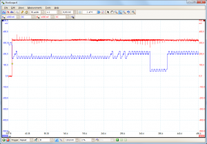
On the left you can see a short piece of SPI communications as seen by the oscilloscope through the D/A converter (blue trace). I have wired the clock signal to least significant bit (input 1) so it causes the smallest level change. MOSI, MISO and CS are the three other lines.
I initially did the calibration and logic level conversion by capturing waveforms in the oscilloscope software, saving them as .CSV files and running custom C code to create a calibration files and logic levels out of them. I modified my SD tutorial firmware a bit to toggle additional pin when data was being sent, and used that on the second oscilloscope channel (red trace) to trigger capture.
However, the Picoscope 2000 series has a nice C API which also offers access to the fast streaming option, and also eliminates one step in the capture process. So I made a simple calibration program to save the logic levels into a text file, and capture programs to get reading from scope, convert them back to logic using those levels, and save into format understood by the OLS (Open Logic Sniffer).
After a bit of testing, I managed to get the streaming capture program to work reliably at 2.5 MSps (faster capture rates did not work on my scope/PC combo). The other capture program included only captures a single buffer, but can operate at any capture rate supported by the scope, but is of course limited by scope buffer size. Capture rates above 1 MSps were enough to ensure error-free capture of SPI communications done around 200 kHz (5 samples or more per logic state).
You can get my sample programs and try them out yourself if you have a compatible 2000 series PicoScope. A word of warning: This is not a finalized end product, but a proof of concept implementation that requires a solid grasp of C fundamentals if you want to adapt it to your needs. For experienced programmers it should be really straightforward and easy to understand. The code provided above is currently licensed under GPL. Due to licensing terms, I have not included parts of the Picoscope SDK to my project zip – you need to download it here and copy PS2000.h, DLL and LIB files to the project directory yourself.
Possible further developments for this project could include:
- Integrating the D/A/D -conversion trick to OLS, Sigrok or a similar project
- Modifying the code to support “frequency” recognition so length of original logic levels would be more accurately preserved (current implementation discards most of the length hints)
- Graphical mode
- Realtime triggering based on logic level conversion – could be easily implemented as part of the streaming capture program
- SPI analysis and other serial protocol analysis “on the fly” – the capture program could directly output interpreted serial traffic instead of just logic levels
I hope you found this post useful! I’d be interested in all comments and ideas regarding this project. Also, if you think this is cool, feel free to link back. :)
