Level Shifting 101
While writing my FAT+SD tutorial, I realized that my projects may soon contain both 3.3 V components like an SD card, and 5.0 V components like LCD displays or a MAX232 UART chip. Considering I only knew how to use resistors as voltage dividers, I decided to learn a bit more about voltage level shifting.
Having netted already two generous donations for this blog, I decided to spend the first one on $10 of components that could do the job, and employ my trusty, although not old, Picoscope 2205 to investage how they perform!
Simple low to high conversion: Flexible logic levels
When interfacing a 3.3V device with an AVR chip running at 5V, it is possible that no shifting is needed when communicating to the AVR chip. For example, the ATtiny13 datasheet specifies input low voltage as anything less than 0.3*VCC (1.5V when VCC=5V) and high as anything more than 0.7*VCC (3.5V when VCC=5V) – the 3.3V might be just enough to be reliably interpreted as “high” in your particular part combo. However, you might still want to consider the alternatives below, just to be sure.
Simple high to low conversion: Voltage dividers
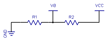
The basic trick for lowering a voltage from, say 5V to 3.3V is to use two resistors in series, connected between the MCU pin and the ground. Because the voltage drop in each is proportional to the ohm value of each resistor, it’s easy to get any voltage between MCU VCC and ground from such a setup.
Basically, V0 = R1 / (R1+R2) * VCC. For example, if your MCU is providing 5V when an output pin is set high, you could have a 2k resistor (R2) and 3k resistor (R1) in series, resulting in 3V between the two resistors – that is because the 2k resistor “consumes” 2/5 of the overall voltage (5V->3V) and 3k resistor 3/5 of the voltage (3V->0V).
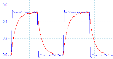
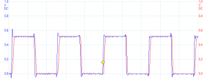
To see how it works in reality, I made a voltage divider from two 10k resistors, and measured both the voltage on MCU pin itself (the blue trace) and from between the two resistors (the red trace), when the MCU pin is set to alternate between low and high state 200 000 times a second (a 100 kHz square wave):
Such a setup works quite nicely for low frequencies and high impedance inputs (i.e. the circuit connected to V0 draws a lot less current than the R1 resistor). However, when the signal frequency increases, the setup starts to “round” the edges of the signal – here’s the same setup near 1 MHz:
Update: The reason for this behavior is that the breadboard traces between the resistors and even oscilloscope probes have a small amount of capacitance, which generates a low-pass filter that starts to distort (or dampen) the high frequency signals. It’s like there was a tiny capacitor added between the resistors. Also, no actual resistor is ideal, so even the resistors themselves have a tiny amount of capacitance. Thanks for Ross McKenzie from ValuSoft for pointing this out!
It’s not hard to image such a poor square wave would cause communication problems between circuits. Lowering the resistor values to 1k fixes this problem, but still the shape of transition is a bit round (and it already draws around 1mA of current):
Also, voltage divider doesn’t help if we’d like to shift voltage from 3V to 5V. It’s time for some alternatives.
4050B quad buffer
The first level shifting part is the 4050 hex non-inverting buffer. The “hex” part means there’s actually six separate buffers in one chip, much like there’s four in the parts with “quad” in their description. The Fairchild’s 4050B datasheet explicitly states in the part introduction:
These devices feature logic level conversion using only one supply voltage (VDD). The input signal high level (VIH) can exceed the VDD supply voltage when these devices are used for logic level conversions.
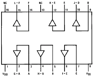
So basically, you can power the 4050 with 3.3V voltage, but provide 5V logic at its input, effectively transforming the simple buffer into high->low voltage shifter. The pinout is also very simple: there are six inputs (A-F) and six corresponding outputs (G-L) which replicate the logical high/low states of the inputs and the outputs (but on the circuit’s voltage levels, high=VDD, low=VSS). Only additional connections are the operating voltage (VDD) and ground (VSS).
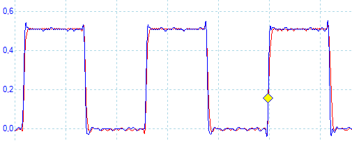
After wiring the 4050B to a breadboard, I plugged the ATtiny2313 generating a 820 kHz square wave into one of its inputs (blue trace) and measured the signal at the output (red trace). Note that both ATtiny and 4050B are run from same voltage here, so no level shifting is actually done in this instance.
The waveform looks very good with hardly any delay when compared to the original trace. We can conclude that at least around 1 MHz, the 4050B is an excellent choice for high->low voltage shifting.
4104B quad low-to-high voltage translator
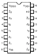
This part is only one of the many buffers that can do the shifting the other way around – from low to high, for example from 3.3V to 5V. Like many similar parts, it features dual voltage supplies: VDDI for input, and VDDO for output. Also common for this type of part, the VDDI voltage should never exceed VDDO – note that this means you should always wire VDDO before VDDI!
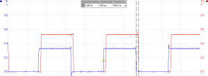
This particular part sports dual outputs for each input – both the logical value and its complement are available. The outputs can also be switched off to a high impedance state by taking the “output enable” (EO) pin low. This time I wired the part to both 3.3V (input) and 5V (output), and fed a 300 kHz square wave to one of the inputs (click for the full size version):
Appearing here for the first time in noticeable magnitude is the property called propagation delay – the time it takes before a logic level change at input is reflected on the output level. With 4104B and my particular setup, the delay was 130 ns (nanoseconds) – my Picoscope software allows me to measure that easily (see the image). If you look at the datasheet, the typical and maximum values for different transitions at different voltages are prominently listed, and it’s one of the key values for these types of components.
Why is the propagation delay important? Consider a 1 MHz square wave. One waveform spends 500 ns in high state and 500 ns in low state – if this was a clock signal from 3.3V master to 5V slave, the slave would see the rising edge 26 % later than the master (relative to the length of the clock high state). With any additional delays (e.g. in high->low voltage conversion), the communication between the devices might not work at all. Unless I was some way sure the delay in a specific case would not be a problem, I’d avoid any situation where the propagation delay is more than a few percent of the wavelength. With 130 ns, this would mean a maximum communication frequency of about 150 kHz.
HCF 40109 B quad low to high voltage level shifter
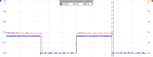
This part is very similar to the 4104B, but the datasheet highlights a few key differences: Each buffer has a separate output enable pin that must be high to activate the output. Also, this particular part can also work as high to low level shifter, as output supply voltage can be less than input supply voltage. It also means the one can connect the power supplies in either order, unlike with the 4104B. However, this feature comes at a price: the propagation delay is longer, especially in the high to low transition – it’s clearly visible even when the square wave frequency is lowered to 40 kHz (at 800 kHz, the output hardly had time to get down before the next rise):
At 480 ns, the propagation delay limits the use of this circuit to low frequency signal switching. It’s also shows why you might want to check the propagation delay from datasheet before purchasing a component for a particular purpose.
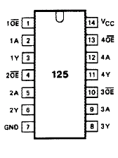
74HCT125 quad tri-state buffer
Two voltage shifting parts recommended in Adafruit’s microSD tutorial (where I actually started this journey) were 74AHC125 and 74LVX245. Neither were available from my local electronics supply, but 74HCT125 was, and I read that the “T” in 74HCT series comes from the fact that it’s compatible with TTL logic levels, i.e. a voltage of 3V would be interpreted as “high” even when the part is run from a 5V supply. So much like the previous 40109 part, it might be usable for 3.3V -> 5V shifting. It also has separate “output enable” pins for each output, switching the output between low impedance and high impedance state.
Additional note considering the 74HCT series was that unused inputs should not be left “floating”, which could dramatically increase its power consumption, but instead either connected to GND or VCC. Also, some source said that it cannot source much current, so if you’re lighting LEDs to see if the thing works, connect the LED and a resistor between output pin and VCC, not GND. This way the output will sink current, something it should be better at (of course, the LED will now light when output is LOW…).
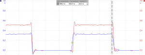
So I wired the 74HCT125 to 5V supply, connected then “1A” input pin to my 3.3V “square wave generator” and measured the results. It worked perfectly, and turned out the propagation delay was hardly even visible, even at full 820 kHz speed (I actually think that my power supply, probe calibration and ATtiny2313 waveform produce more artifacts than the 125 here):
So while it’s not actually designed for voltage shifting, it does 3.3V -> 5V shifting quite nicely!
Conclusions
Armed with a 10 MHz oscilloscope and poor mans (almost) 1 MHz square wave generator, I was able to evaluate the suitability of four different IC’s for voltage shifting tasks. My testing also showed that in addition to the voltage characteristics, the propagation delay is a critical attribute to consider in any signalling applications above 100 kHz.
And considering I picked my test sample from a local electronics store, I also became quite convinced that it’s not too hard to get such parts when the need arises – with the exception of perhaps the 40109, all of them easily met my rather low-speed signalling needs. So even if these particular ones are not available, look at the other 4000 and 74HCT/AHC/LXV series buffers, and you’ll likely find what you’re looking for.
I hope you enjoyed the post. As always, feel free to suggest any new topics in the comments!
